1. Crystal Framework and Split Anisotropy
1.1 The 2H and 1T Polymorphs: Structural and Electronic Duality
(Molybdenum Disulfide)
Molybdenum disulfide (MoS TWO) is a split shift metal dichalcogenide (TMD) with a chemical formula including one molybdenum atom sandwiched in between 2 sulfur atoms in a trigonal prismatic sychronisation, forming covalently bound S– Mo– S sheets.
These private monolayers are piled vertically and held together by weak van der Waals pressures, enabling very easy interlayer shear and peeling down to atomically slim two-dimensional (2D) crystals– an architectural attribute central to its varied functional roles.
MoS ₂ exists in several polymorphic forms, the most thermodynamically stable being the semiconducting 2H phase (hexagonal proportion), where each layer displays a direct bandgap of ~ 1.8 eV in monolayer type that transitions to an indirect bandgap (~ 1.3 eV) wholesale, a sensation vital for optoelectronic applications.
In contrast, the metastable 1T phase (tetragonal proportion) adopts an octahedral sychronisation and behaves as a metal conductor due to electron donation from the sulfur atoms, enabling applications in electrocatalysis and conductive compounds.
Stage shifts between 2H and 1T can be caused chemically, electrochemically, or through strain engineering, providing a tunable system for making multifunctional devices.
The capability to stabilize and pattern these phases spatially within a solitary flake opens up pathways for in-plane heterostructures with distinctive digital domains.
1.2 Defects, Doping, and Side States
The efficiency of MoS ₂ in catalytic and digital applications is highly sensitive to atomic-scale issues and dopants.
Innate factor flaws such as sulfur openings act as electron contributors, boosting n-type conductivity and functioning as active websites for hydrogen development responses (HER) in water splitting.
Grain borders and line defects can either restrain cost transportation or create localized conductive paths, depending upon their atomic setup.
Controlled doping with shift metals (e.g., Re, Nb) or chalcogens (e.g., Se) enables fine-tuning of the band structure, carrier concentration, and spin-orbit combining results.
Notably, the sides of MoS two nanosheets, especially the metal Mo-terminated (10– 10) sides, display considerably higher catalytic activity than the inert basal aircraft, inspiring the design of nanostructured drivers with made best use of side exposure.
( Molybdenum Disulfide)
These defect-engineered systems exhibit exactly how atomic-level adjustment can change a naturally taking place mineral into a high-performance useful product.
2. Synthesis and Nanofabrication Techniques
2.1 Mass and Thin-Film Production Approaches
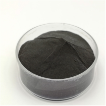
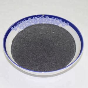
All-natural molybdenite, the mineral kind of MoS TWO, has been used for decades as a solid lubricant, but modern-day applications demand high-purity, structurally managed synthetic types.
Chemical vapor deposition (CVD) is the dominant method for generating large-area, high-crystallinity monolayer and few-layer MoS ₂ films on substratums such as SiO TWO/ Si, sapphire, or versatile polymers.
In CVD, molybdenum and sulfur forerunners (e.g., MoO five and S powder) are vaporized at heats (700– 1000 ° C )under controlled environments, allowing layer-by-layer development with tunable domain name size and positioning.
Mechanical exfoliation (“scotch tape approach”) stays a benchmark for research-grade examples, generating ultra-clean monolayers with marginal problems, though it lacks scalability.
Liquid-phase peeling, entailing sonication or shear mixing of mass crystals in solvents or surfactant solutions, generates colloidal diffusions of few-layer nanosheets ideal for coatings, compounds, and ink formulas.
2.2 Heterostructure Assimilation and Gadget Pattern
Truth potential of MoS two emerges when incorporated right into upright or side heterostructures with other 2D products such as graphene, hexagonal boron nitride (h-BN), or WSe ₂.
These van der Waals heterostructures make it possible for the style of atomically accurate tools, including tunneling transistors, photodetectors, and light-emitting diodes (LEDs), where interlayer fee and power transfer can be crafted.
Lithographic patterning and etching methods enable the manufacture of nanoribbons, quantum dots, and field-effect transistors (FETs) with network sizes down to tens of nanometers.
Dielectric encapsulation with h-BN protects MoS ₂ from environmental destruction and decreases charge scattering, considerably improving carrier wheelchair and tool stability.
These manufacture breakthroughs are vital for transitioning MoS ₂ from research laboratory interest to practical part in next-generation nanoelectronics.
3. Practical Qualities and Physical Mechanisms
3.1 Tribological Habits and Strong Lubrication
Among the earliest and most enduring applications of MoS ₂ is as a dry solid lubricant in extreme atmospheres where liquid oils fail– such as vacuum, heats, or cryogenic problems.
The reduced interlayer shear strength of the van der Waals space allows simple moving between S– Mo– S layers, resulting in a coefficient of rubbing as reduced as 0.03– 0.06 under ideal conditions.
Its performance is additionally enhanced by strong attachment to steel surfaces and resistance to oxidation up to ~ 350 ° C in air, beyond which MoO five formation enhances wear.
MoS ₂ is widely utilized in aerospace systems, vacuum pumps, and gun parts, usually used as a finish by means of burnishing, sputtering, or composite incorporation right into polymer matrices.
Recent studies show that moisture can break down lubricity by increasing interlayer bond, triggering research into hydrophobic layers or crossbreed lubes for enhanced environmental security.
3.2 Electronic and Optoelectronic Feedback
As a direct-gap semiconductor in monolayer kind, MoS ₂ exhibits strong light-matter interaction, with absorption coefficients exceeding 10 five cm ⁻¹ and high quantum return in photoluminescence.
This makes it suitable for ultrathin photodetectors with fast action times and broadband sensitivity, from visible to near-infrared wavelengths.
Field-effect transistors based upon monolayer MoS two demonstrate on/off proportions > 10 ⁸ and provider movements up to 500 centimeters TWO/ V · s in put on hold examples, though substrate communications normally limit useful worths to 1– 20 centimeters ²/ V · s.
Spin-valley combining, a consequence of solid spin-orbit interaction and broken inversion balance, makes it possible for valleytronics– an unique paradigm for info encoding using the valley level of freedom in momentum area.
These quantum phenomena placement MoS ₂ as a prospect for low-power logic, memory, and quantum computing components.
4. Applications in Power, Catalysis, and Emerging Technologies
4.1 Electrocatalysis for Hydrogen Evolution Reaction (HER)
MoS ₂ has emerged as an appealing non-precious alternative to platinum in the hydrogen development reaction (HER), a crucial process in water electrolysis for eco-friendly hydrogen production.
While the basal plane is catalytically inert, edge sites and sulfur openings exhibit near-optimal hydrogen adsorption totally free energy (ΔG_H * ≈ 0), comparable to Pt.
Nanostructuring approaches– such as producing up and down aligned nanosheets, defect-rich movies, or doped hybrids with Ni or Carbon monoxide– make best use of active site thickness and electric conductivity.
When integrated into electrodes with conductive sustains like carbon nanotubes or graphene, MoS two accomplishes high current thickness and lasting stability under acidic or neutral problems.
More improvement is accomplished by stabilizing the metallic 1T phase, which boosts inherent conductivity and subjects added energetic websites.
4.2 Versatile Electronic Devices, Sensors, and Quantum Tools
The mechanical flexibility, transparency, and high surface-to-volume proportion of MoS two make it suitable for flexible and wearable electronic devices.
Transistors, reasoning circuits, and memory devices have actually been shown on plastic substrates, allowing bendable display screens, wellness monitors, and IoT sensors.
MoS TWO-based gas sensing units show high sensitivity to NO TWO, NH ₃, and H ₂ O due to charge transfer upon molecular adsorption, with feedback times in the sub-second array.
In quantum innovations, MoS two hosts local excitons and trions at cryogenic temperatures, and strain-induced pseudomagnetic areas can trap providers, making it possible for single-photon emitters and quantum dots.
These growths highlight MoS two not just as a useful material however as a platform for exploring fundamental physics in minimized dimensions.
In summary, molybdenum disulfide exhibits the merging of classical materials science and quantum engineering.
From its old function as a lube to its modern implementation in atomically slim electronics and power systems, MoS two continues to redefine the borders of what is feasible in nanoscale materials style.
As synthesis, characterization, and assimilation techniques development, its influence throughout science and modern technology is positioned to expand also better.
5. Provider
TRUNNANO is a globally recognized Molybdenum Disulfide manufacturer and supplier of compounds with more than 12 years of expertise in the highest quality nanomaterials and other chemicals. The company develops a variety of powder materials and chemicals. Provide OEM service. If you need high quality Molybdenum Disulfide, please feel free to contact us. You can click on the product to contact us.
Tags: Molybdenum Disulfide, nano molybdenum disulfide, MoS2
All articles and pictures are from the Internet. If there are any copyright issues, please contact us in time to delete.
Inquiry us